370_4046 VCO & PLL FUNCTIONS

Quote from Defran on October 4, 2026, 7:32 am
The 4046 is a widely used analog-digital integrated circuit containing a Phase-Locked Loop (PLL). Its function is to generate a signal and adjust its frequency until it synchronizes with an input signal. It also includes an independent voltage-controlled oscillator (VCO) within the same package.
- The VCO (Voltage-Controlled Oscillator): produces a square wave. Its frequency changes based on the voltage applied to its control input.
- The two phase comparators: compare the input signal with the VCO signal and generate a correction signal; these comparators can be selected via an external switch:Comparator I (Exclusive-OR): Works well with input signals having a symmetrical duty cycle (50%) and moderate noise.
Comparator II (Sequential / Edge Detector): A digital circuit sensitive to rising edges. It functions even if the signal's duty cycle is not 50% and offers a wider lock range.The Phase-Locked Loop (PLL):
By connecting the VCO output—either directly or through a frequency divider—back to the phase comparator, the system automatically adjusts the VCO voltage until its frequency and phase exactly match those of an external reference signal.Here is how the system works:
1. The comparator detects the difference between the two signals.
2. An external filter smooths the correction signal to produce a control voltage.
3. This voltage adjusts the VCO frequency.
4. Once the circuit locks, the VCO tracks the input frequency and maintains a stable phase relationship.The VCO can be used standalone—without closing the PLL loop—as a square-wave generator where the frequency is controlled by the voltage at the SIGNAL IN pin.
It belongs to the CMOS logic family (4000 series), and its typical applications include:
- Frequency Demodulation (FM): Extracts audio or data information from a frequency-modulated signal.
- Frequency Multipliers and Dividers: Generates frequencies that are exact multiples of an input clock signal.
- Frequency Synthesizers: A traditional basis for generating multiple stable frequencies from a reference oscillator (crystal).
- Tone Decoding: Detects the presence of a specific frequency within a composite signal (e.g., in DTMF telephone dialing systems).
- Clock Recovery: Recovers the clock signal from an asynchronous digital data stream.Commercialy, it is available as CD4046, HC4046 and so on, depending on the manufacturer.
Key Electrical Characteristics:
Maximum VCO frequency: It can oscillate from a few hertz to several megahertz (typically up to 1 MHz or 2 MHz, depending on the supply voltage). In our case, this limitation is tied to the simulator's own operation.
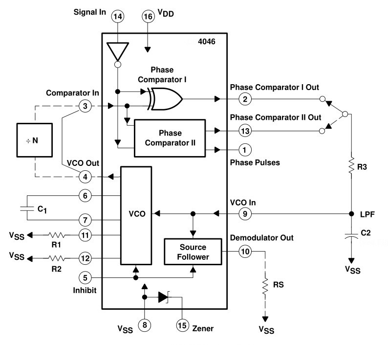
INTERNAL BLOCK DIAGRAM:
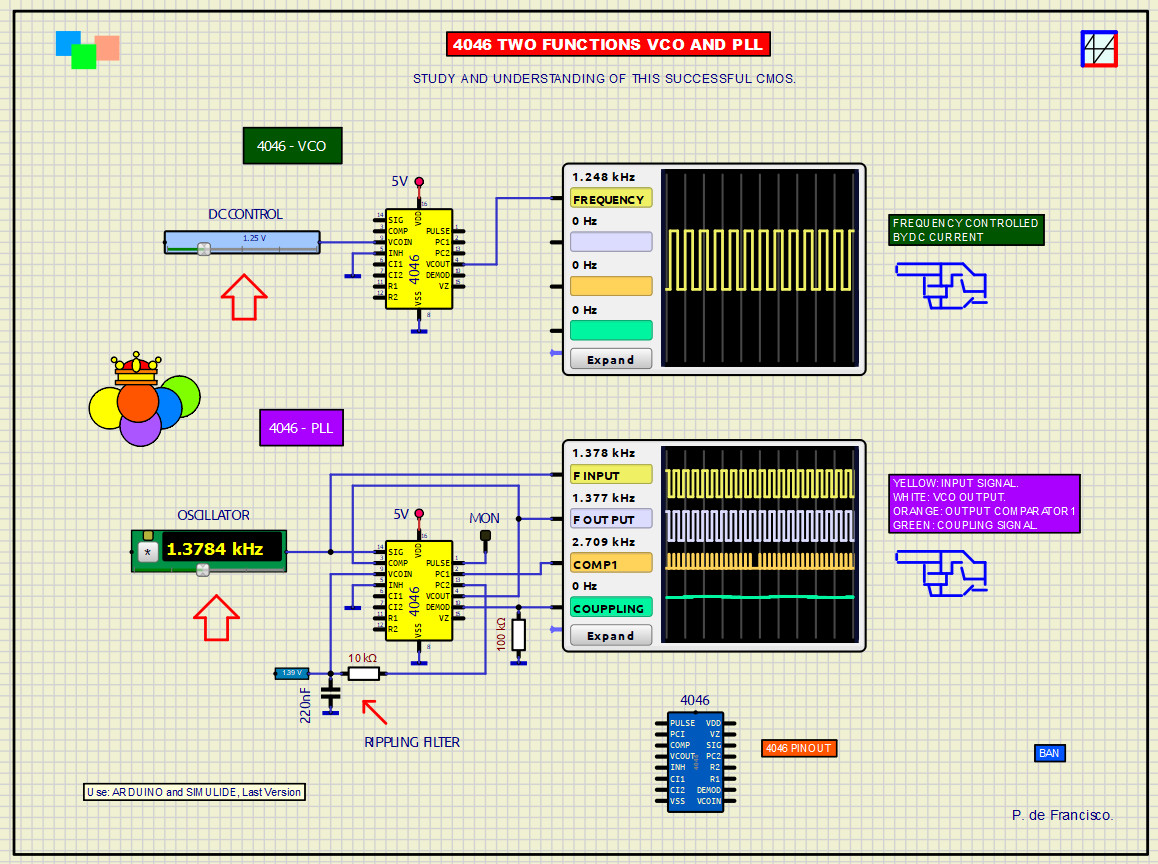
In our example, changing the input frequency causes the output to self-adjust until it is in phase with the input. The modulator signals and the phase of the phase comparator II pulses are also visible.
SCRIPT PROGRAM:
Including the files *.as, *. mcu and *.package
// 4046 - MODELO FUNCIONAL. DEFRAN26
// VCO: 0..5 V de control => 0..5 kHz con VDD = 5 V.
// PC1: XOR. PC2: detector de flancos con salida de tres estados.
// PULSE: indicador simplificado de diferencia de fase (no pin 1 exacto).
// DEMOD: pin 10, seguidor ideal de la tension de control VCOIN.
// Paso interno: 1 us = 1000000 ps.

IoPin@ sigPin = component.getPin("SIG");
IoPin@ compPin = component.getPin("COMP");
IoPin@ vinPin = component.getPin("VCOIN");
IoPin@ inhPin = component.getPin("INH");
IoPin@ vddPin = component.getPin("VDD");
IoPin@ vssPin = component.getPin("VSS");
IoPin@ vcoPin = component.getPin("VCOOUT");
IoPin@ pc1Pin = component.getPin("PC1");
IoPin@ pc2Pin = component.getPin("PC2");
IoPin@ pulsePin = component.getPin("PULSE");
IoPin@ demodPin = component.getPin("DEMOD");
bool oldSig = false;
bool oldComp = false;
bool up = false;
bool down = false;
bool vcoState = false;
double phase = 0.0;
int pc2Mode = -1;

void setup()
{
  print("4046: modelo cargado");
}

void setPC2(int mode, double low, double high)
{
  // mode: 0 = alta impedancia, 1 = bajo, 2 = alto.
  if (mode != pc2Mode)
  {
    if (mode == 0) pc2Pin.setPinMode(1);
    else pc2Pin.setPinMode(3);
    pc2Mode = mode;
  }
  if (mode == 1) pc2Pin.setVoltage(low);
  if (mode == 2) pc2Pin.setVoltage(high);
}

void reset()
{
  component.cancelEvents();
  sigPin.setPinMode(1);
  compPin.setPinMode(1);
  vinPin.setPinMode(1);
  inhPin.setPinMode(1);
  vddPin.setPinMode(1);
  vssPin.setPinMode(1);
  vcoPin.setPinMode(3);
  pc1Pin.setPinMode(3);
  pulsePin.setPinMode(3);
  demodPin.setPinMode(3);
  pc2Mode = -1;
  setPC2(0, 0.0, 5.0);
  vcoPin.setVoltage(0);
  pc1Pin.setVoltage(0);
  pulsePin.setVoltage(0);
  demodPin.setVoltage(0);
  phase = 0.0;
  vcoState = false;
  oldSig = false;
  oldComp = false;
  up = false;
  down = false;
  component.addEvent(1000000);
  print("4046: eventos iniciados");
}

void runEvent()
{
  double low = vssPin.getVoltage();
  double high = vddPin.getVoltage();
  double supply = high - low;
  if (supply < 1.0)
  {
    phase = 0.0;
    vcoState = false;
    up = false;
    down = false;
    oldSig = false;
    oldComp = false;
    vcoPin.setVoltage(low);
    pc1Pin.setVoltage(low);
    pulsePin.setVoltage(low);
    demodPin.setVoltage(low);
    setPC2(0, low, high);
    component.addEvent(1000000);
    return;
  }
  double threshold = low + supply * 0.5;
  double control = (vinPin.getVoltage() - low) / supply;
  if (control < 0.0) control = 0.0;
  if (control > 1.0) control = 1.0;
  // DEMOD: salida analogica del control del VCO, pin 10.
  demodPin.setVoltage(low + supply * control);
  // Rango normalizado: frecuencia = 5000 * control Hz.
  if (inhPin.getVoltage() >= threshold || control <= 0.0)
  {
    phase = 0.0;
    vcoState = false;
  }
  else
  {
    phase += 2.0 * 5000.0 * control * 0.000001;
    if (phase >= 1.0)
    {
      phase -= 1.0;
      vcoState = !vcoState;
    }
  }
  if (vcoState) vcoPin.setVoltage(high);
  else vcoPin.setVoltage(low);
  bool sig = sigPin.getVoltage() >= threshold;
  bool comp = compPin.getVoltage() >= threshold;
  if (sig != comp) pc1Pin.setVoltage(high);
  else pc1Pin.setVoltage(low);
  if (sig && !oldSig) up = true;
  if (comp && !oldComp) down = true;
  if (up && down)
  {
    up = false;
    down = false;
  }
  if (up) setPC2(2, low, high);
  else if (down) setPC2(1, low, high);
  else setPC2(0, low, high);
  if (up || down) pulsePin.setVoltage(high);
  else pulsePin.setVoltage(low);
  oldSig = sig;
  oldComp = comp;
  component.addEvent(1000000);
}
EXAMPLE FILES:
The compressed ZIP file contains all parts of the example and subcircuits. If you wish to create the 4046 component in Simulide, follow the steps for including it as a subcircuit as described in the Simulide tutorials and add it to the MENU in the corresponding XML file.
P. de Francisco.
The 4046 is a widely used analog-digital integrated circuit containing a Phase-Locked Loop (PLL). Its function is to generate a signal and adjust its frequency until it synchronizes with an input signal. It also includes an independent voltage-controlled oscillator (VCO) within the same package.
- The VCO (Voltage-Controlled Oscillator): produces a square wave. Its frequency changes based on the voltage applied to its control input.
- The two phase comparators: compare the input signal with the VCO signal and generate a correction signal; these comparators can be selected via an external switch:
Comparator I (Exclusive-OR): Works well with input signals having a symmetrical duty cycle (50%) and moderate noise.
Comparator II (Sequential / Edge Detector): A digital circuit sensitive to rising edges. It functions even if the signal's duty cycle is not 50% and offers a wider lock range.
The Phase-Locked Loop (PLL):
By connecting the VCO output—either directly or through a frequency divider—back to the phase comparator, the system automatically adjusts the VCO voltage until its frequency and phase exactly match those of an external reference signal.
Here is how the system works:
1. The comparator detects the difference between the two signals.
2. An external filter smooths the correction signal to produce a control voltage.
3. This voltage adjusts the VCO frequency.
4. Once the circuit locks, the VCO tracks the input frequency and maintains a stable phase relationship.
The VCO can be used standalone—without closing the PLL loop—as a square-wave generator where the frequency is controlled by the voltage at the SIGNAL IN pin.
It belongs to the CMOS logic family (4000 series), and its typical applications include:
- Frequency Demodulation (FM): Extracts audio or data information from a frequency-modulated signal.
- Frequency Multipliers and Dividers: Generates frequencies that are exact multiples of an input clock signal.
- Frequency Synthesizers: A traditional basis for generating multiple stable frequencies from a reference oscillator (crystal).
- Tone Decoding: Detects the presence of a specific frequency within a composite signal (e.g., in DTMF telephone dialing systems).
- Clock Recovery: Recovers the clock signal from an asynchronous digital data stream.
Commercialy, it is available as CD4046, HC4046 and so on, depending on the manufacturer.
Key Electrical Characteristics:
Maximum VCO frequency: It can oscillate from a few hertz to several megahertz (typically up to 1 MHz or 2 MHz, depending on the supply voltage). In our case, this limitation is tied to the simulator's own operation.
INTERNAL BLOCK DIAGRAM:
In our example, changing the input frequency causes the output to self-adjust until it is in phase with the input. The modulator signals and the phase of the phase comparator II pulses are also visible.
SCRIPT PROGRAM:
Including the files *.as, *. mcu and *.package
// 4046 - MODELO FUNCIONAL. DEFRAN26
// VCO: 0..5 V de control => 0..5 kHz con VDD = 5 V.
// PC1: XOR. PC2: detector de flancos con salida de tres estados.
// PULSE: indicador simplificado de diferencia de fase (no pin 1 exacto).
// DEMOD: pin 10, seguidor ideal de la tension de control VCOIN.
// Paso interno: 1 us = 1000000 ps.

IoPin@ sigPin = component.getPin("SIG");
IoPin@ compPin = component.getPin("COMP");
IoPin@ vinPin = component.getPin("VCOIN");
IoPin@ inhPin = component.getPin("INH");
IoPin@ vddPin = component.getPin("VDD");
IoPin@ vssPin = component.getPin("VSS");
IoPin@ vcoPin = component.getPin("VCOOUT");
IoPin@ pc1Pin = component.getPin("PC1");
IoPin@ pc2Pin = component.getPin("PC2");
IoPin@ pulsePin = component.getPin("PULSE");
IoPin@ demodPin = component.getPin("DEMOD");
bool oldSig = false;
bool oldComp = false;
bool up = false;
bool down = false;
bool vcoState = false;
double phase = 0.0;
int pc2Mode = -1;

void setup()
{
  print("4046: modelo cargado");
}

void setPC2(int mode, double low, double high)
{
  // mode: 0 = alta impedancia, 1 = bajo, 2 = alto.
  if (mode != pc2Mode)
  {
    if (mode == 0) pc2Pin.setPinMode(1);
    else pc2Pin.setPinMode(3);
    pc2Mode = mode;
  }
  if (mode == 1) pc2Pin.setVoltage(low);
  if (mode == 2) pc2Pin.setVoltage(high);
}

void reset()
{
  component.cancelEvents();
  sigPin.setPinMode(1);
  compPin.setPinMode(1);
  vinPin.setPinMode(1);
  inhPin.setPinMode(1);
  vddPin.setPinMode(1);
  vssPin.setPinMode(1);
  vcoPin.setPinMode(3);
  pc1Pin.setPinMode(3);
  pulsePin.setPinMode(3);
  demodPin.setPinMode(3);
  pc2Mode = -1;
  setPC2(0, 0.0, 5.0);
  vcoPin.setVoltage(0);
  pc1Pin.setVoltage(0);
  pulsePin.setVoltage(0);
  demodPin.setVoltage(0);
  phase = 0.0;
  vcoState = false;
  oldSig = false;
  oldComp = false;
  up = false;
  down = false;
  component.addEvent(1000000);
  print("4046: eventos iniciados");
}

void runEvent()
{
  double low = vssPin.getVoltage();
  double high = vddPin.getVoltage();
  double supply = high - low;
  if (supply < 1.0)
  {
    phase = 0.0;
    vcoState = false;
    up = false;
    down = false;
    oldSig = false;
    oldComp = false;
    vcoPin.setVoltage(low);
    pc1Pin.setVoltage(low);
    pulsePin.setVoltage(low);
    demodPin.setVoltage(low);
    setPC2(0, low, high);
    component.addEvent(1000000);
    return;
  }
  double threshold = low + supply * 0.5;
  double control = (vinPin.getVoltage() - low) / supply;
  if (control < 0.0) control = 0.0;
  if (control > 1.0) control = 1.0;
  // DEMOD: salida analogica del control del VCO, pin 10.
  demodPin.setVoltage(low + supply * control);
  // Rango normalizado: frecuencia = 5000 * control Hz.
  if (inhPin.getVoltage() >= threshold || control <= 0.0)
  {
    phase = 0.0;
    vcoState = false;
  }
  else
  {
    phase += 2.0 * 5000.0 * control * 0.000001;
    if (phase >= 1.0)
    {
      phase -= 1.0;
      vcoState = !vcoState;
    }
  }
  if (vcoState) vcoPin.setVoltage(high);
  else vcoPin.setVoltage(low);
  bool sig = sigPin.getVoltage() >= threshold;
  bool comp = compPin.getVoltage() >= threshold;
  if (sig != comp) pc1Pin.setVoltage(high);
  else pc1Pin.setVoltage(low);
  if (sig && !oldSig) up = true;
  if (comp && !oldComp) down = true;
  if (up && down)
  {
    up = false;
    down = false;
  }
  if (up) setPC2(2, low, high);
  else if (down) setPC2(1, low, high);
  else setPC2(0, low, high);
  if (up || down) pulsePin.setVoltage(high);
  else pulsePin.setVoltage(low);
  oldSig = sig;
  oldComp = comp;
  component.addEvent(1000000);
}
EXAMPLE FILES:
The compressed ZIP file contains all parts of the example and subcircuits. If you wish to create the 4046 component in Simulide, follow the steps for including it as a subcircuit as described in the Simulide tutorials and add it to the MENU in the corresponding XML file.
P. de Francisco.
Uploaded files: