
363__THE IC 74x595 AND LED EFFECTS PRACTICE
Quote from Defran on March 29, 2024, 10:40 am
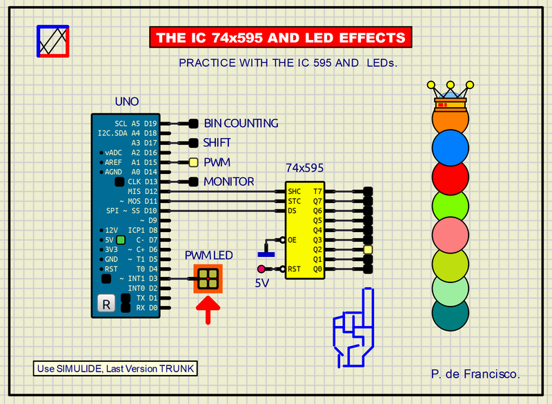
363__THE IC 74x595 AND LED EFFECTS PRACTICE. (Simulide R2259 or Higher).
The 74X595 integrated circuit is widely used in UNO to increase the number of outputs. Here we use it to obtain an eight-bit binary counter. Also on an LED we establish a PWM up and down sequence. Functionally everything is in sequence to form the practice.SCHEME:
Four LEDs connected to D13, D15, D17 and D19 act as sequence monitors. The IC 74x595 is an octuple register with serial input and eight outputs stored in parallel, typically used to increase the number of outputs, it occupies only three of the controller: D10, DS for data, D11, STC for the parallel storage pulse and D12, SHC for serial charging. On D3 there is an LED to show the PWM ramps.
To Know more about the IC 74x595: https://www.diodes.com/assets/Datasheets/74HC595.pdf
PROGRAM:
This is a program in which you can clearly see each of its functions, highlighting only the specific instructions for handling 74x595: shiftOut(dataP, clockP, MSBFIRST, Num);
// THE IC 74x595 AND LED EFFEECTS PRACTICE. DEFRAN24. int count=19; int shift=17; int Lpwm=15; int mon=13; int clockP=12; // SHC of 595, Clock int latchP=11; // STC of 595, Latch int dataP=10; // DS of 595, Data int pwm=3; void setup() { pinMode(latchP, OUTPUT); pinMode(clockP, OUTPUT); pinMode(dataP, OUTPUT); analogWrite(count, OUTPUT); analogWrite(shift, OUTPUT); analogWrite(Lpwm, OUTPUT); pinMode(mon, OUTPUT); analogWrite(pwm, 0); digitalWrite(mon, HIGH); delay(300); digitalWrite(mon, LOW);delay(300); digitalWrite(mon, HIGH); delay(300); digitalWrite(mon, LOW);delay(300); digitalWrite(mon, HIGH); delay(300); digitalWrite(mon, LOW);delay(300); } void loop() { byte b=0x01; for (int i=0; i<8; i++) { digitalWrite(shift, HIGH); delay(100); digitalWrite(latchP, LOW); // Latch data shiftOut(dataP, clockP, MSBFIRST, b); // shift data digitalWrite(latchP, HIGH); // latch data digitalWrite(shift, LOW); delay(100); digitalWrite(Lpwm, HIGH); for (int v=0; v<255; v++) // FADE high { analogWrite(pwm, v); delay(12); } for (int v=255; v>0; v--) // FADE low { analogWrite(pwm, v); delay(10); } digitalWrite(Lpwm, LOW); b=b << 1; } digitalWrite(count, HIGH); for (int Num=0; Num<256; Num++) // count 0 to 255 { digitalWrite(latchP, LOW); // latch low shiftOut(dataP, clockP, MSBFIRST, Num); // shift digitalWrite(latchP, HIGH); // latch high delay(300); } digitalWrite(count, LOW); }SUBCIRCUITS:This example integrates several subcircuits located in the "data" folder into the ZIP attached. This folder must always be next to the "sim1" scheme so that it can be executed. A subcircuit is a “custom” circuit that accumulates a set of Simulide base components (primitive function) to obtain a new or an adapted function. These subcircuits are treated by Simulide as another component of its own structure. User can create his own subcircuits or use the ones published here in your own designs once the procedure is known, explained in detail in the Simulide tutorials: https://simulide.com/p/subcircuits/* Communication with the author: Simulide/User/Messages/DefranP. de Francisco.
363__THE IC 74x595 AND LED EFFECTS PRACTICE. (Simulide R2259 or Higher).
SCHEME:
Four LEDs connected to D13, D15, D17 and D19 act as sequence monitors. The IC 74x595 is an octuple register with serial input and eight outputs stored in parallel, typically used to increase the number of outputs, it occupies only three of the controller: D10, DS for data, D11, STC for the parallel storage pulse and D12, SHC for serial charging. On D3 there is an LED to show the PWM ramps.
To Know more about the IC 74x595: https://www.diodes.com/assets/Datasheets/74HC595.pdf
PROGRAM:
This is a program in which you can clearly see each of its functions, highlighting only the specific instructions for handling 74x595: shiftOut(dataP, clockP, MSBFIRST, Num);
// THE IC 74x595 AND LED EFFEECTS PRACTICE. DEFRAN24.

int count=19;
int shift=17;
int Lpwm=15;
int mon=13;
int clockP=12;  // SHC of 595, Clock
int latchP=11;  // STC of 595, Latch
int dataP=10;   // DS  of 595, Data
int pwm=3;

void setup()
{
  pinMode(latchP, OUTPUT);
  pinMode(clockP, OUTPUT);
  pinMode(dataP, OUTPUT);
  analogWrite(count, OUTPUT);
  analogWrite(shift, OUTPUT);
  analogWrite(Lpwm, OUTPUT);
  pinMode(mon, OUTPUT);
  analogWrite(pwm, 0);
  digitalWrite(mon, HIGH); delay(300); digitalWrite(mon, LOW);delay(300);
  digitalWrite(mon, HIGH); delay(300); digitalWrite(mon, LOW);delay(300);
  digitalWrite(mon, HIGH); delay(300); digitalWrite(mon, LOW);delay(300);
}

void loop()
{
  byte b=0x01;
  for (int i=0; i<8; i++)
  {
    digitalWrite(shift, HIGH);
    delay(100);
    digitalWrite(latchP, LOW);             // Latch data
    shiftOut(dataP, clockP, MSBFIRST, b);  // shift data
    digitalWrite(latchP, HIGH);            // latch data
    digitalWrite(shift, LOW);
    delay(100);
    digitalWrite(Lpwm, HIGH);
    for (int v=0; v<255; v++)              // FADE high
    {
      analogWrite(pwm, v);
      delay(12);
    }
    for (int v=255; v>0; v--)               // FADE low
    {
      analogWrite(pwm, v);
      delay(10);
    }
    digitalWrite(Lpwm, LOW);
    b=b << 1;
  }
  digitalWrite(count, HIGH);
  for (int Num=0; Num<256; Num++)            // count 0 to 255
  {
    digitalWrite(latchP, LOW);               // latch low
    shiftOut(dataP, clockP, MSBFIRST, Num);  // shift
    digitalWrite(latchP, HIGH);              // latch high
    delay(300);
  }
  digitalWrite(count, LOW);
}