DS18B20-39 Ds18b20::command : Warning: ROM command Not implemented
Quote from SiR on October 15, 2025, 10:08 amI have been having trouble to resolve this. I think the ROM command refers to the skip ROM command.
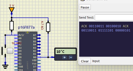
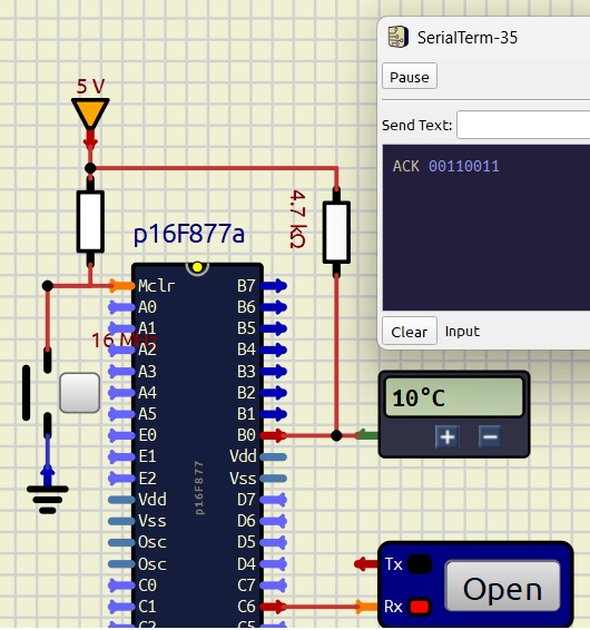
The circuit is as shown and I've included the relevant codes. I also output each step to a uart terminal to show if the program is running as expected. I hope someone can help me troubleshoot this.
The codes are built on MPLAP X IDE assembly language in the attached text file.
DELAY_A equ 0x70
DELAY_MULTIPLIER equ 0x71 ;variable for the multiplier
cmd_addr equ 0x72 ;variable for the ROM command address
Mms_MULTIPLIER equ 0x74 ; this variable is to store the required inner iteration steps for delay.
bit_counter equ 0x75 ; variable for the counting the number of bits that are being sent
byte_recd equ 0x76 ; variable for storing the read byte
byte_recd_1 equ 0x77 ; variable for storing byte 1 of the LSB of the converted temperaturemain:
call reset_pulse ; step1 initialization
call rom_skip_cmd ; step2 issue skip cmd.
goto mainreset_pulse:
call PIC_bus_rx ; To start in rx mode
call PIC_bus_tx ; pull the bus low for tx
call delay_480us
call PIC_bus_rx ; release the bus
call delay_60us ; wait for the bus to pull high
call delay_10us ; wait for DS to pull the bus low
call register_DS_presence
call delay_480us
returnregister_DS_presence:
bcf STATUS,5 ; now, bank0
btfsc PORTB,0
goto send_NACK
call send_ACK
returnPIC_bus_tx:
bsf STATUS,5 ; bank1 is selected by assigning 1 to bit 5 and bit 6=0 by default 01
movlw 0x00 ; assigns B0 as output
movwf TRISB ; set PORTD as input pins
bcf STATUS,5 ; now, bank0
bcf PORTB,0
return
PIC_bus_rx:
bsf STATUS,5 ; bank1 is selected by assigning 1 to bit 5 and bit 6=0 by default 01
movlw 0x01 ; assigns B0 as input
movwf TRISB ; set PORTB as input pins
bcf STATUS,5 ; now, bank0
bcf PORTB,0
return; ==== write command byte ===========
rom_skip_cmd:
call init_var
call PIC_bus_rx ; release the bus first
write_Byte:
btfss cmd_addr,0
goto write_0
write_1:
call PIC_bus_tx ; pull the bus low for tx
call delay_1us
call PIC_bus_rx ; release the bus, i.e. turn to Rx mode
call delay_60us ; and hold that for at least 60us
call send_bit_1
goto next_bit
write_0:
call PIC_bus_tx ; pull the bus low for tx
call delay_60us ; and hold that for at least 60us
call PIC_bus_rx ; release the bus, i.e. turn to Rx mode
call send_bit_0
next_bit:
decfsz bit_counter
goto shift_bit
goto start_function_cmd
shift_bit:
rrf cmd_addr,1 ; right shift of the register bit
goto write_Byte ; go check if the new bit zero is '1' or '0'
;========================================
start_function_cmd:
call send_space
return; ==== variables initialisation ============
init_var:
movlw 0x08 ; assign 8 to W
movwf bit_counter ; assign 8 bits to the counter
movlw 0xCC ; assign 204 to W
movwf cmd_addr ; assign the register to the skip command register
bcf STATUS,0
return
; === delay modules ==========================
delay_193us: ; total delay time is about 192s
movf Mms_MULTIPLIER,0 ; put Mms_MULTIPLIER to W
movwf DELAY_A ; move the Mms_MULTIPLIER from W
delay_a: ; this line is executed after the movwf DELAY_A
decfsz DELAY_A,1 ;value in DELAY_A=DELAY_A-1 and skip if DELAY_A=0.
; The 1 indicates that the decremented value is put back to DELAY_A
goto delay_a ; keep the decrement process; if value in DELAY_A=0, this goto line is skipped
return ; and this return line is executed. It returns to the next line when the call insx was executed.
delay_480us:
movlw 0xFF ; delay a total of 480us with 255+255+135 as the value of Mms_MULTIPLIER
movwf Mms_MULTIPLIER ; 255
call delay_193us ; delay 193us
call delay_193us ; delay another 193us
movlw 0x87 ; 135
movwf Mms_MULTIPLIER
call delay_193us ; delay another 103us, therefore 193x2+103=489us
return
delay_10us:
movlw 0x0A ; delay 10us with 10 as the value of Mms_MULTIPLIER
movwf Mms_MULTIPLIER ; 10
call delay_193us ; delay 193us
return
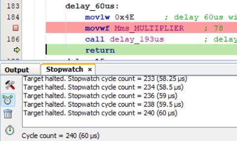
delay_60us:
movlw 0x0A ; delay 60us with 78 as the value of Mms_MULTIPLIER
movwf Mms_MULTIPLIER ; 10
call delay_193us ; delay 193us
return
delay_1us:
nop
nop
nop
nop
return
I have been having trouble to resolve this. I think the ROM command refers to the skip ROM command.
The circuit is as shown and I've included the relevant codes. I also output each step to a uart terminal to show if the program is running as expected. I hope someone can help me troubleshoot this.
The codes are built on MPLAP X IDE assembly language in the attached text file.
DELAY_A equ 0x70
DELAY_MULTIPLIER equ 0x71 ;variable for the multiplier
cmd_addr equ 0x72 ;variable for the ROM command address
Mms_MULTIPLIER equ 0x74 ; this variable is to store the required inner iteration steps for delay.
bit_counter equ 0x75 ; variable for the counting the number of bits that are being sent
byte_recd equ 0x76 ; variable for storing the read byte
byte_recd_1 equ 0x77 ; variable for storing byte 1 of the LSB of the converted temperature
main:
call reset_pulse ; step1 initialization
call rom_skip_cmd ; step2 issue skip cmd.
goto main
reset_pulse:
call PIC_bus_rx ; To start in rx mode
call PIC_bus_tx ; pull the bus low for tx
call delay_480us
call PIC_bus_rx ; release the bus
call delay_60us ; wait for the bus to pull high
call delay_10us ; wait for DS to pull the bus low
call register_DS_presence
call delay_480us
return
register_DS_presence:
bcf STATUS,5 ; now, bank0
btfsc PORTB,0
goto send_NACK
call send_ACK
return
PIC_bus_tx:
bsf STATUS,5 ; bank1 is selected by assigning 1 to bit 5 and bit 6=0 by default 01
movlw 0x00 ; assigns B0 as output
movwf TRISB ; set PORTD as input pins
bcf STATUS,5 ; now, bank0
bcf PORTB,0
return
PIC_bus_rx:
bsf STATUS,5 ; bank1 is selected by assigning 1 to bit 5 and bit 6=0 by default 01
movlw 0x01 ; assigns B0 as input
movwf TRISB ; set PORTB as input pins
bcf STATUS,5 ; now, bank0
bcf PORTB,0
return
; ==== write command byte ===========
rom_skip_cmd:
call init_var
call PIC_bus_rx ; release the bus first
write_Byte:
btfss cmd_addr,0
goto write_0
write_1:
call PIC_bus_tx ; pull the bus low for tx
call delay_1us
call PIC_bus_rx ; release the bus, i.e. turn to Rx mode
call delay_60us ; and hold that for at least 60us
call send_bit_1
goto next_bit
write_0:
call PIC_bus_tx ; pull the bus low for tx
call delay_60us ; and hold that for at least 60us
call PIC_bus_rx ; release the bus, i.e. turn to Rx mode
call send_bit_0
next_bit:
decfsz bit_counter
goto shift_bit
goto start_function_cmd
shift_bit:
rrf cmd_addr,1 ; right shift of the register bit
goto write_Byte ; go check if the new bit zero is '1' or '0'
;========================================
start_function_cmd:
call send_space
return
; ==== variables initialisation ============
init_var:
movlw 0x08 ; assign 8 to W
movwf bit_counter ; assign 8 bits to the counter
movlw 0xCC ; assign 204 to W
movwf cmd_addr ; assign the register to the skip command register
bcf STATUS,0
return
; === delay modules ==========================
delay_193us: ; total delay time is about 192s
movf Mms_MULTIPLIER,0 ; put Mms_MULTIPLIER to W
movwf DELAY_A ; move the Mms_MULTIPLIER from W
delay_a: ; this line is executed after the movwf DELAY_A
decfsz DELAY_A,1 ;value in DELAY_A=DELAY_A-1 and skip if DELAY_A=0.
; The 1 indicates that the decremented value is put back to DELAY_A
goto delay_a ; keep the decrement process; if value in DELAY_A=0, this goto line is skipped
return ; and this return line is executed. It returns to the next line when the call insx was executed.
delay_480us:
movlw 0xFF ; delay a total of 480us with 255+255+135 as the value of Mms_MULTIPLIER
movwf Mms_MULTIPLIER ; 255
call delay_193us ; delay 193us
call delay_193us ; delay another 193us
movlw 0x87 ; 135
movwf Mms_MULTIPLIER
call delay_193us ; delay another 103us, therefore 193x2+103=489us
return
delay_10us:
movlw 0x0A ; delay 10us with 10 as the value of Mms_MULTIPLIER
movwf Mms_MULTIPLIER ; 10
call delay_193us ; delay 193us
return
delay_60us:
movlw 0x0A ; delay 60us with 78 as the value of Mms_MULTIPLIER
movwf Mms_MULTIPLIER ; 10
call delay_193us ; delay 193us
return
delay_1us:
nop
nop
nop
nop
return
Quote from arcachofo on October 15, 2025, 10:22 amHi.
Maybe you can explain what is exactly the problem.
Also share the files needed to reproduce the problem: .sim1, .asm and .hex
You can zip the files and attach to your post.
Hi.
Maybe you can explain what is exactly the problem.
Also share the files needed to reproduce the problem: .sim1, .asm and .hex
You can zip the files and attach to your post.
Quote from SiR on October 16, 2025, 1:46 amHi,
The problem is I'm not reading the correct temperature. It doesn't look like the DS18B20 is responding after these commands
reset->skip->T convert then reset->skip->read scratchpad.
Please find the attached information as requested.
Thanks & regards
Hi,
The problem is I'm not reading the correct temperature. It doesn't look like the DS18B20 is responding after these commands
reset->skip->T convert then reset->skip->read scratchpad.
Please find the attached information as requested.
Thanks & regards
Uploaded files:
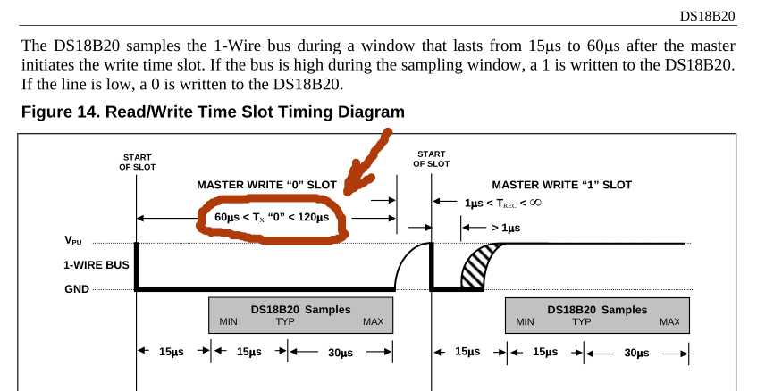
Quote from arcachofo on October 16, 2025, 2:25 pmSeems that all low pulses are below 15 us, so all the bits are read as 1, a 0 should be a low pulse > 30 us
I think you should check your delay_60us routine.
Seems that all low pulses are below 15 us, so all the bits are read as 1, a 0 should be a low pulse > 30 us
I think you should check your delay_60us routine.
Quote from SiR on October 17, 2025, 3:47 amThanks you very much for the reply. Yes, I had realized the parameter for the delay_60us is incorrect and corrected it. And the warning message has now disappeared. However, I'm still getting the same reading of the first returned byte, i.e. 11111111.
I've double check the data sheet of DS18B20. It seems to me that the master sample should be taken around 15us for both read 0 and read 1. The slave should 0 and 1 accordingly. May I clarify this " low pulses are below 15 us, so all the bits are read as 1, a 0 should be a low pulse > 30 us"
Thanks you very much for the reply. Yes, I had realized the parameter for the delay_60us is incorrect and corrected it. And the warning message has now disappeared. However, I'm still getting the same reading of the first returned byte, i.e. 11111111.
I've double check the data sheet of DS18B20. It seems to me that the master sample should be taken around 15us for both read 0 and read 1. The slave should 0 and 1 accordingly. May I clarify this " low pulses are below 15 us, so all the bits are read as 1, a 0 should be a low pulse > 30 us"
Uploaded files:
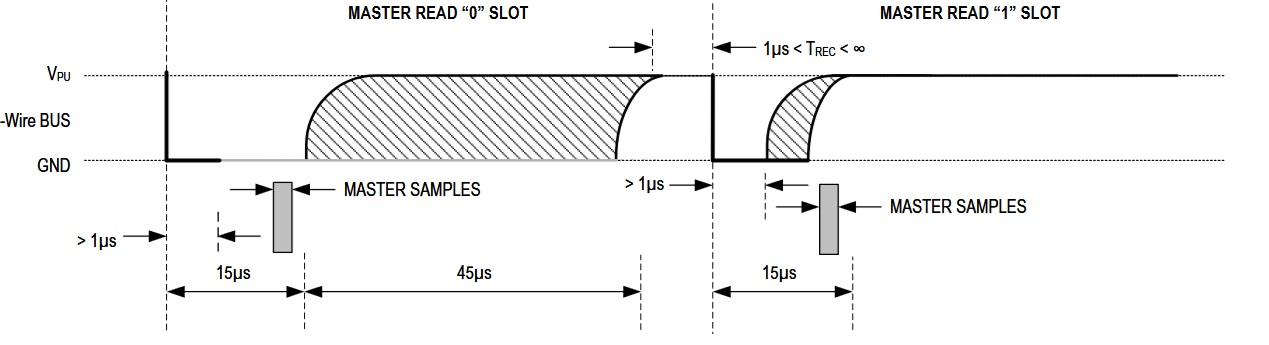
Quote from arcachofo on October 17, 2025, 7:52 amYou are right about the master sample, but here we are talking about DS18B20 sample (master writing).
In the datasheet you see that the time for a "0" should be > 60 us, in real devices lower times might work, so simulide uses 30 us which is the "typical" (TYP):
You are right about the master sample, but here we are talking about DS18B20 sample (master writing).
In the datasheet you see that the time for a "0" should be > 60 us, in real devices lower times might work, so simulide uses 30 us which is the "typical" (TYP):
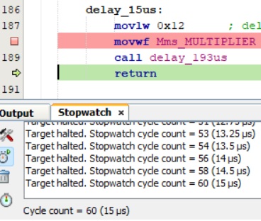
Quote from SiR on October 17, 2025, 10:15 amIn my 2nd zip attachment, I've already corrected the delay_60us when master is writing. The message of "Warning: ROM command Not implemented" has gone but still reading 11111111 as the first byte after read scratchpad functional cmd. I've also verified the delay_60us and delay_15us modules with the MPLAB X software. The issue now seems to be with the simulide not returning the 0 and/or 1 as per the DS18B20 read time 0 and read time 1 datasheet. Or am I missing something?
In my 2nd zip attachment, I've already corrected the delay_60us when master is writing. The message of "Warning: ROM command Not implemented" has gone but still reading 11111111 as the first byte after read scratchpad functional cmd. I've also verified the delay_60us and delay_15us modules with the MPLAB X software. The issue now seems to be with the simulide not returning the 0 and/or 1 as per the DS18B20 read time 0 and read time 1 datasheet. Or am I missing something?
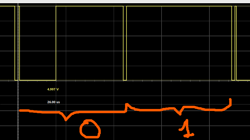
Quote from arcachofo on October 17, 2025, 11:06 amIt must be some other problem in your firmware, DS18B20 is sending 0xA0 as the first byte.
"0" is sent as a 25 us low pulse after 1 us of master read slot.
So if you read at 15 us you should get (LSB first): 0 0 0 0 1 0 1
It must be some other problem in your firmware, DS18B20 is sending 0xA0 as the first byte.
"0" is sent as a 25 us low pulse after 1 us of master read slot.
So if you read at 15 us you should get (LSB first): 0 0 0 0 1 0 1
Quote from SiR on October 18, 2025, 6:22 amYes, there was indeed another problem in the code after I had gone through the read_byte module again. I need to re-initialize the bit_counter variable in the beginning of this module. It does work after that. Thanks you very much for your help.
Yes, there was indeed another problem in the code after I had gone through the read_byte module again. I need to re-initialize the bit_counter variable in the beginning of this module. It does work after that. Thanks you very much for your help.